In the hyper-competitive world of the solar industry, manufacturers are always on the lookout for better performing raw materials and technology that can accelerate power output. Performance is something that gives them a competitive edge on other players.
The last decade has seen a momentous growth in solar-powered products. The undying quest of manufacturing a superlative module without altering the manufacturing techniques brought new formats of solar wafers in the market.
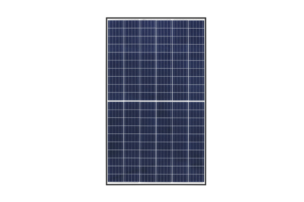
In the last few years, PV tech has undergone tremendous changes and brought new innovations such as half-cut panels, PERC technology, multi bus bar designs and the major shift to monocrystalline wafers from multi-crystalline one. These ingenious developments are pushing high-quality and high-efficiency products into mainstream markets to gain a foothold.

The sneak peek in the past
Did you know that the first module with a power rating of 48watts was introduced in 1983? It had 36 cells with 100X100 mm wafers – they dominated the market for almost 13 years. Thereafter, a manufacturer in the US brought panels with a power rating of 120 watts with 125 X125 mm wafers. Later, they persisted as the standard size for many years.
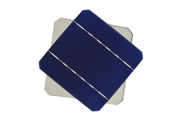
Finally, the manufacturers started using type M0 wafers in modules – this size 156mm X 156mm (from a 200 mm diameter ingot) had been the most dominant and popular in the semiconductor industry for almost 10 years.
The new era of PV tech industry
Ultimately, M0 was successively substituted by M2, M3, M4, M6 and M12 type variants with 60, 72 and 144 solid solar cell panels. M2 was launched by a Chinese PV manufacturer. Until 2018, they constituted more than 90% of the market – in both mono and multi-crystalline wafer.
The sole reason behind switching to larger wafer sizes is the huge production cost as compared to the overall capacity. After the advent of countless wafer sizes from M0 to M12 on the marketplace, the old models became obsolete.
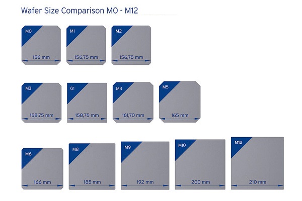
Gone are the days when these dimensions were a standard in the solar market, now new wafer sizes are being introduced every year. As manufacturers have begun to move ahead, they are now trying to maximize the active space available on the module to meet the modern demands for panels with higher power ratings. In the year 2019 alone, 3 wafer sizes were introduced – M3, M4 and M6.
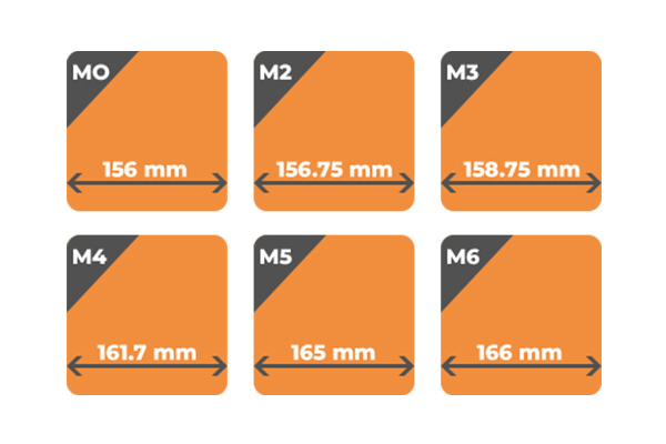
In M3 format wafer, the size has increased by 2mm and the dimension is 158.75 X 158.75mm. In this scenario, it is crucial to inform you that only the panel size increases due to the use of twin-cell technology. The wafer sizes of M4 and M6 are 161.7 mm and 166mm. To stay ahead in the industry, some companies have even started introducing the M12 format in 210mm size. Usually, they were measured in inches but presently millimetre depicts the wafer size.
Benefits of larger wafer sizes
All these new formats of wafers strengthen the module power by giving a crucial boost for a competitive cost per watt – they curtail the production cost. Besides that, the ultimate goal is to lower the balance of systems cost by accommodating more watts in the same racking system. The larger wafer size enables the production of more semiconductor components with only one wafer which results in higher productivity and efficiency of wafers.
M4 format
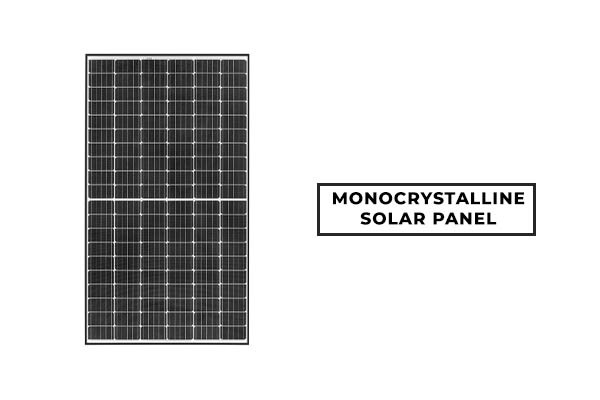
This format is predominantly used by EPC companies that offer premium quality modules with exceptional efficiency. They consider it the most cost-efficient option on the market, as they utilize the ingot better than the M2 wafers which help boost module power by 20-25 watts by minimizing the labour and support material cost during the installation process.
M6 format
As per Longi, the M6 wafer can boost the overall power output by 8%. It also declared that the M6 wafer minimizes the costs at both cell and module level by $0.007/W and shrinks the investment on parts such as racking, cabling, and racking system.
In bigger modules, every array needs a few brackets and these brackets also require more steel to support the large structure. Thus, the bracket cost is cut down and so the cost decreases notably with the size of power rating. It can be adopted without much disruption in the production line.
Way Forward
It is still a matter of debate as to which wafer size should be the new standard. The larger the sizes of wafers, the more disrupted the old manufacturing units will be. For instance – the M12 format can challenge the supply chain and downstream market.
However, the industry is trying to find ways to balance the equation – a wafer size that optimizes the module manufacturing process without adding complexity to the installation process.
With the shifting requirements of the manufacturers and customers, it is certain that the marketplace will not accept modules with lower power ratings. And since boosting power output by incorporating larger wafers seems like a reasonable way, it is highly likely that it will witness a widespread adoption.
With that, M2 may soon become a thing of the past. There are also predictions that the market share of the M6 format will be more than 50% in 2020 and can reach up to 70% by 2021. And that will set the course for other players in the market – their adoption will determine the industry size in the coming future.
Novergy has always brought new solar innovations and has evolved with the changing requirements of diversification and standardization. If you are planning to invest in solar, explore our newly added half-cut modules, Bifacial, BIPV with the latest technology (PERC) and designs (5-busbar). We have spent the last 13+ years perfecting our products to ensure maximum output.
Visit novergysolar.com and check out our solar solutions now!

